Saturday 27 June 2015

Basic and useful information's about multiroters

The level of interest in multi-rotor aircraft has increased dramatically in the past couple of years. There have been heaps of noob posts in this forum in the past few months, and it seems that good information is spread out over many threads and can be hard to find. The purpose of this thread is to help people who have little or no multi-rotor (or RC) experience to buy the right equipment and successfully get an aircraft into the air. Hopefully this guide will de-mystify the process and help people through the process of selecting suitable components which work well together. 
If the concept of building an aircraft from scratch scares you, then you're probably in the wrong thread.
What are all these parts for?
A brief explanation of what all the major parts do: 
Frame - the structural component of your aircraft, keeping everything where it belongs. All of your components will be connected to your frame in some way. 

Control board - the "brains" that keeps your aircraft steady in the air, and translates the pilot’s commands into movement. It uses various sensors and a micro-processor to determine what your aircraft is doing, and makes adjustments to the aircraft’s motor speeds to keep it controllable. 

Radio receiver - Receives commands from the pilot’s radio and relays them to the aircraft’s control board. 

Motor and propeller - create thrust and lift from stored electrical energy. 

Electronic Speed Controller (ESC) - convert DC power from the battery to AC power to the motors. By varying the current and timing of electrical pulses, the speed of the motor can be changed. 

Battery - the source of electrical power for all the other components. The size of the battery can vary widely, depending on the number of motors, the size of the motors, the weight of any payload and the flight time desired. 

Power distribution board - a simple circuit board which makes connecting multiple ESC’s wiring to the same battery simple and neat. This can also be made from cables, particularly for large aircraft with high current. Some frames have power distribution circuitry built into the frame.


What are you trying to do?
The very first step in building a multi-rotor aircraft should be to decide what you want it to be able to do. Some people just want to fly around, some want to carry cameras or other payloads, some want to do aerobatics, some want to build an automated drone aircraft. An aerobatic aircraft will not be very good at carrying a heavy payload, and vice versa. So you need to make this decision first - all of your component selections will depend on this decision.


Pick your brains
The next step is to determine which control board your aircraft will use. The control board is the "brains" that will keep your aircraft steady in the air, and translate your commands into movement. Control boards range from basic control boards to very expensive boards with autopilot, advanced self-stabilisation and camera gimbal controls costing several hundred dollars.
I'd recommend the KK 2.0 control board to begin with. It's relatively cheap , it can be configured for various motor configurations, it has sufficient sensors to be reasonably stable out of the box, and it has a built-in setup routine on an LCD screen to walk you through the setup process.


Keeping it together
Next, we'll need to select a frame. Frames need to be strong enough to withstand the forces of opposing motors without flexing and cope with rough landings without breaking. Meanwhile, it must also be light enough that your motors can easily lift it, and ideally have a small aerodynamic profile to avoid being too affected by wind. Frames may also be required to dampen vibration, or to support a camera or other equipment. 
Your frame selection will depend on what you want your aircraft to do. For the sake of simplicity, I’ve assumed you’re going for a 4-motor craft, commonly referred to as a quadcopter. 


Picking powerplants 
This is a big subject and rather long-winded, so please bear with me. 
Choosing the right motor is important for good performance in any aircraft, but it’s particularly critical in a multi-rotor aircraft where your aircraft is literally hanging in the air, suspended under rotors. With the sheer number of motors available, and the array of different sizes, speeds and specifications for each motor, choosing suitable motors can be a daunting task. 
To begin the basic selection process, we need to how much thrust will be required to keep the craft in the air. The basic rule of thumb with multi-rotors is that your motors should be capable of producing twice the total flying weight of your craft in thrust. This “safety margin” ensures that your motors will be capable of responding quickly to your control inputs, or arresting a rapid vertical descent, even when your battery voltage is reduced over time. 
Our equation is therefore as follows: required thrust per motor = ( Aircraft weight x 2 ) / 4 motors
So for a 4-motor craft, each motor must be capable of producing half the aircraft’s weight in thrust.
No doubt you’re already seeing the problem with this equation – you don’t actually know what your aircraft will weigh yet! Fortunately we can make some educated guesses to get us in the ballpark. For the purpose of estimation, we can assume that each motor and its accompanying propeller weighs 100 grams – a total of 400 grams for 4 motors. Add the weight of the frame, which is likely to be around 450-500 grams. Add another 300 grams for the battery, and another 100 grams for the 4 ESC’s and their wiring & plugs. And your radio receiver, control board and wiring will probably weigh another 50 grams or so. If you’re carrying a payload, such as a camera or other special equipment, you’ll need to add that as well. 
For the average quadcopter, the total flying weight is likely to be around 1.3kg. Using the equation above, we now know we’re looking for a total thrust of 2.6kg, or 650g per motor. We now know we’re looking for motors weighing up to 100 grams, which can generate at least 650 grams of thrust using a 3-cell battery and a propellor of 8-12 inches diameter (see more on this below). 
For aerobatic aircraft, you should be looking at motors of around 1000-1400kV and relatively small propellers. These will make your aircraft more responsive and allow flips and other aerobatic manoeuvres, at the expense of being a little more difficult to control.
For larger multi-rotors, or aircraft carrying payloads, large propellers and low-kv motors work best. These have more rotational momentum, and will more easily maintain your aircraft’s stability. Look for 700-900kv motors capable of making the thrust you need.
You’re now ready to start looking for motors. The list of specifications for each motor on HobbyKing can be daunting, but try to check for the following items on each motor:
1. Weight - 100 grams or less
2. Voltage - 3-cell (11.1V) generally what you’re looking for
3. Motor speed (kV) - choose according to the speed guidelines above
4. Thrust data - this is sometimes missing from the product description, but can often be found in the reviews or comments. Look for thrust data for the voltage and prop size as per the guidelines above.


Choosing a speed controller
Once you've picked out the motor you will use, you also need to select the Elecrotronic Speed Controller (ESC) that will run it. Thankfully, this task is much simpler than motor selection. 
ESCs are primarily rated for the amount of current they can constantly supply to the motor. Some may also have a "burst current" rating, but this should be ignored for now. Determine the maximum current draw from your chosen motor's specifications. Add a 10% safety margin, and look for ESCs rated for at least this amount of current. You will also need to check that your chosen ESC is rated for the correct number of battery cells (usually 3 cells or 11.V) and ensure that it's not too heavy. Once again, any excess weight will be quadrupled, since you need 4 of these items. 
Be aware that you need 4 identical ESCs for your aircraft. It's possible to make a quadcopter fly with 4 different ESCs, but it will be more erratic and much harder to control.


Propellers
It's a pretty simple job to select propellers, in theory. The specifications for your motor should indicate roughly what size you need, to create the thrust you're seeking. However, there are a few complications.
The main issue is finding propellers which are available in both standard and counter-rotating arrangements. Multi-rotors have half the motors spinning clockwise (CW), and the other half will be spinning counter-clockwise (CCW) - thus effectively balancing out each other's torque for a stable equilibrium. To make it easier for you, HobbyKing sell a variety of sizes of propellers in CW and CCW bundles, ranging from 5" all the way up to 13" diameter. 
Each of your new propellers need to be balanced before they're used on your aircraft. Slight flaws in the casting process mean that one blade of your propeller can be slightly heavier than the other, creating a vibration when the propeller is spinning quickly.


Battery
When choosing a battery, the two main things to be concerned with are capacity and weight. On the face of it, it seems simple - a battery with a greater capacity will keep your aircraft in the air for longer.
However, batteries with greater capacity are also heavier, which means your motors need to work harder to keep the aircraft in the air. You may end up getting a shorterflight time from a larger battery, if you're not careful.
The method I used to decide which battery to use is relatively simple. My motor-choice rule of thumb is to have twice as much thrust as my aircraft weighs. Since the battery is the last main (heavy) component I'm selecting, I now have a pretty good idea how much thrust I will have, and how much weight I can afford to add. So I simply add up the weight of all my components and payload (minus the unknown battery) and calculate how much "spare" thrust I have to achieve the 2:1 thrust to weight ratio. I can then find a 3-cell battery of around that weight - easy.
As a starting point for your search, I'd suggest a 3S battery with a capacity of around 2700-3000mah. You may need to adjust that to suit your aircraft's weight and thrust. I personally recommend using Turnigy NanoTech batteries, because they have a good C rating and have excellent weight/capacity ratio.


Other electrical components
There are a couple of other electrical-related items needed for a complete multi-rotor aircraft - these are explained in greater detail below. 

power distribution board is often used to make connecting 4 sets of ESC wires together in a neat and orderly manner. Power distribution boards are usually a simple circuit board with 2 tracks, one for positive wires and one for negative wires.

low battery alarm is another vital piece of equipment for any multi-rotor aircraft. This small item monitors your battery's voltage, and sounds an alarm when it drops below a certain amount.

Radio transmitter and receiver
Having a multi-rotor isn't much fun if you can't control it. You're going to need to have wireless communication with your aircraft to steer it in the right directions. If you already have a 4-channel (or more) radio, all you will need for your new multi-rotor is a spare 4-channel (or more) receiver, preferably a compact lightweight one. If you have additional channels, you may wish to control additional functions on the control board, such as auto-pilot or RTH if your board supports this, or to trigger lights, operate a camera or toggle a bomb drop.
Monday 16 March 2015

Op-Amp IC’s – Pin Configuration, Features & Working

 IC 741

The most commonly used op-amp is IC741. The 741 op-amp is a voltage amplifier, it inverts the input voltage at the output, can be found almost everywhere in electronic circuits.

Pin Configuration:

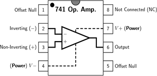
Let’s see the pin configuration and testing of 741 op-amps. Usually, this is a numbered counter clockwise around the chip. It is an 8 pin IC. They provide superior performance in integrator, summing amplifier and general feedback applications. These are high gain op-amp; the voltage on the inverting input can be maintained almost equal to Vin.
Pin Configuration of 741 Op-amp Diagram
It is a 8-pin dual-in-line package with a pinout shown above.
Pin 1: Offset null.
Pin 2: Inverting input terminal.
Pin 3: Non-inverting input terminal.
Pin 4: –VCC (negative voltage supply).
Pin 5: Offset null.
Pin 6: Output voltage.
Pin 7: +VCC (positive voltage supply).
Pin 8: No Connection.
The main pins in the 741 op-amp are pin2, pin3 and pin6. In inverting amplifier, a positive voltage is applied to pin2 of the op-amp; we get output as negative voltage through pin 6. The polarity has been inverted. In a non-inverting amplifier, a positive voltage is applied to pin3 of the op-amp; we get output as positive voltage through pin 6. Polarity remains the same in non-inverting amplifier. Vcc is usually in the range from 12 to 15 volts. When two supplies (+Vcc/-Vcc) are used, they are the same voltage and of opposite sign in almost all cases. Remember that the operational amplifier is a high gain, differential voltage amplifier. For a 741 operational amplifier, the gain is at least 100,000 and can be more than a million (1,000,000). That’s an important fact you’ll need to remember as you put the 741 into a circuit.
There are many common application circuits using IC741 op-amp, they are adder, comparator, subtractor, integrator, differentiator and voltage follower.
Below is some example of 741 IC based circuits. However, the 741 is used as a comparator and not an amplifier. The difference between the two is small but significant. Even if used as a comparator the 741 still detects weak signals so that they can be recognized more easily. A comparator is a circuit that compares two input voltages. One voltage is called the reference voltage and the other is called the input voltage. It is a circuit which compares a signal voltage applied at one input of an op-amp with a known reference voltage at the other input. The 741 op-amp has ideal transfer characteristics (output ±Vsat); and the output is changed by increment in the input voltage of 2mV.

LM324

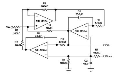
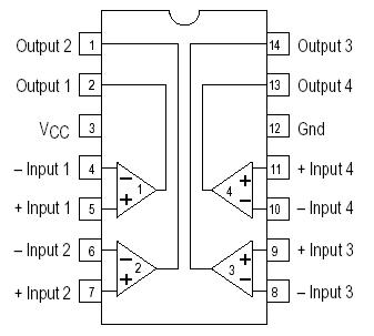
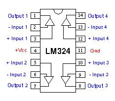
LM324 is a quad op amp integrated circuit with high stability, bandwidth which was designed to operate from a single power supply over a wide range of voltages. They have some dissimilar advantages over standard operational amplifier types in single supply applications. It is a 14-pin dual in-line package, contains four internally compensated and two stage operational amplifiers, shown in figure.


  • Pin 1, 7, 8 and 14 are the outputs of comparator
  • Pin 2, 6, 9 and 13 are the inverting inputs of compactor
  • Pin 3, 5, 10 and 12 are non-inverting inputs of comparator
  • Pin 11 is ground (0V)
  • Pin 4 is supply voltage; 5V
 Features:

Internally frequency compensated for unity gain
Large DC voltage gain 100 dB
Wide bandwidth 1 MHz
Wide power supply range: Single supply 3V to 32V
Essentially independent of supply voltage
Differential input voltage range equal to the power supply voltage
Large output voltage swing 0V to V+ − 1.5V
Potential dividers of LM323 are connected to the inverting and non inverting inputs of the op-amp to give some voltage at these terminals. Supply voltage is given to +V and –V is connected to ground. The output of this comparator will be logic high if the non-inverting terminal input is greater than the inverting terminal input of the comparator. When the inverting input is more than the non-inverting then logic low (0) will be the output.

Working of LM324:

When the power is applied to non-inverting terminal which is less than the inverting voltage of op-amp then the output becomes zero which means there is no current flow. Because we already know that when “+ > – = 1”. Here the ‘+ ‘sign indicates non-inverting terminal and ‘-‘sign indicates the inverting terminal.
If the non-inverting voltage is greater than the inverting voltage then the output will be high.
In this output of LM324 is internally connected to some resistance and it has some arrangement inside the IC, which makes a lot of difference to other comparators.
It is internally pulled-up, so no need of any resistor connection from the supply.


LM339

The LM339 is a most commonly used comparator, designed for use in level detection, low−level sensing and memory applications in automotive and industrial electronic applications. It has four inbuilt comparators; it compares two input voltage levels and gives digital output to show the bigger one.
These comparators additionally have a unique characteristic in that the input common-mode voltage range includes ground, in spite of the fact that they are operated from a single power supply voltage.
  • Pin 1, 2, 13 and 14 are the outputs of comparator
  • Pin 3 is supply voltage; 5V
  • Pin 4, 6, 8 and 10 are inverting inputs of comparator
  • Pin 5, 7, 9 and 11 are non-inverting inputs of comparator
  • Pin 12 is ground; (0V)

Features:

  • Signal or dual supply operation
  • Wide operating supply range (VCC=2V~36V)
    • Max Rating: 2 V to 36 V
    • Tested to 30 V: Non-V Devices
  • Input common-mode voltage includes ground
  • Low supply current drain (IF=0.8mA)
  • Open collector outputs for wired and connection
  • Low input bias current 25nA
  • Low output saturation voltage
  • Output compatible with TTL, DTL, and CMOS logic system
  • Differential input voltage range equal to the power supply voltage
Potential dividers of LM339 are connected to the inverting and non-inverting inputs of the op-amp to give some voltage at these terminals. Supply voltage is given to +V and –V is connected to ground. The output of this comparator will be logic high if the non-inverting terminal input is greater than the inverting terminal input of the comparator.

Working of LM339:

  • When the power is applied to non-inverting terminal which is less than the inverting voltage of op-amp then the output becomes zero which means there is no current flow. Because we already know that when “+ > – = 1”. Here the ‘+ ‘sign indicates non-inverting terminal and ‘-‘sign indicates the inverting terminal.
  • If the non-inverting voltage is greater than the inverting voltage then the current flow will be in the device.
  • The LM339 is act as an open-collector that’s why we connected the resister from the supply, if we remove the resister then there is no current flow in the circuit.


LM358

The LM358 op-amps are used in transducer amplifiers, dc gain blocks and all the conventional op-amp circuits which now can be more easily implemented in single power supply systems. For example, the LM358 op-amp can be directly operated off of the standard +5V power supply voltage which is used as a part of digital systems and will easily provide the required interface electronics without needing the extra ±15V power supplies.
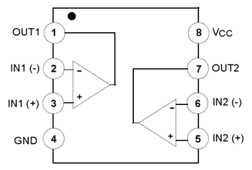
It comes in an 8-pin DIP package is shown in below.

Pin Description:

  • Pin 1 and 7 are outputs of comparator
  • Pin 2 and 6 are inverting inputs
  • Pin 3 and 5 are non-inverting inputs
  • Pin 4 is ground (GND)
  • Pin 8 is VCC+

 Features:

  • Internally frequency compensated for unity gain
  • Large dc voltage gain: 100 DB
  • Wide bandwidth
  • Wide power supply range: single supply: 3V to 32V
  • Very low supply current drain essentially independent of supply voltage
  • Low input offset voltage: 2 mV
  • Input common-mode voltage range includes ground
  • Differential input voltage range equal to the power supply voltage
  • Power drain suitable for battery operation

Advantages:

  • Two internally compensated op amps
  • Eliminates need for dual supplies
  • Allows direct sensing near GND and VOUT also goes to GND
  • Compatible with all forms of logic
  • Power drain suitable for battery operation

Working of LM358:

The inverting input of the comparator LM358 i.e., pin 2 is given to the fixed voltage i.e., in the ratio 47k:10k and the non inverting input of the comparator is pulled down and is given to sensing terminal. When the resistance between the positive supply and the non inverting input is high then resulting is the non-inverting input less than the inverting input making comparator output as logic low at pin1. And when the resistance falls making available a voltage to the non-inverting input higher than inverting input, so that the output of comparator is logic high.


CA 3130 Op Amp

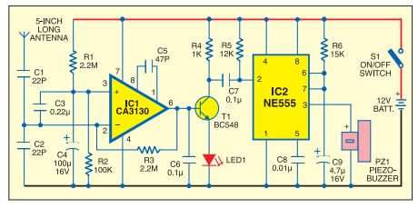
It is excellent Op Amp that requires very low input current requirements. Its output will be in the zero state in the off mode. CA3130 is the 15MHz BiMOS IC with MOSFET inputs and a bipolar output. MOSFET transistors are present in the inputs that provide very high input impedance. The input current can be as low as 10pA. The IC shows very high speed of performance and combines the advantage of both CMOS and bipolar transistors. The presence of PMOS transistors at the inputs results in common mode input voltage capacity down to 0.5 volts below the negative rail. So it is ideal in single supply applications.
The output has CMOS transistor pair that swings the output voltage within 10mV of either supply voltage terminal. IC CA3130 works off 5 to 16 volts and can be phase compensated with a single external capacitor. It also has terminals to adjust the offset voltage and strobing.

CA 3140 Op Amp

It is the 4.5MHz BiMOS Op Amp with MOSFET inputs and bipolar output. It has both PMOS transistors and high voltage bipolar transistors inside. Is inputs have gate protected MOSFETs (PMOS) that provides very high input impedance typically around 1.5T Ohms. The input current requirement is very low around 10pA. It exhibits very fast response and high speed of performance. The output has protection against damage from load terminal shorting. The input stage has PMOS FET which helps in common mode input voltage capability as low as 0.5 volts. The IC is internally phase compensated for stable operation. It also has terminals for additional frequency roll off and offset nulling.


TL071 Op Amp

It is a low noise Op Amp with JFET inputs. It operates in wide common mode and consumes very little current. It requires very low input bias and offset currents. It’s output is short circuit protected and has very high slew rate of 13 V/us and exhibits latch free working.TL0 71 is ideal for high fidelity and audio preamplifier circuits. TL071 and TL0 72 contain only one Op Amp inside while TL074 is a Quad OpAmp with 4 operational amplifiers inside.


TL082 Op Amp

It is a dual OpAmp with separate inputs and outputs. It has JFET inputs and bipolar outputs. The IC shows very high slew rate, low input bias. It also has low offset current and low offset voltage. Its inputs can be biased with very low input currents. Output of the IC is short circuit protected. TL082 exhibits latch free operation and it has the internal frequency compensation.


LM 311 Op Amp

It is a single OPAMP capable of driving DTL, RTL, TTL or MOS circuits. Its output can switch up to 50 volts and 50mA current. It works on wide range of supply voltages from 5 to 30 volts and requires only single supply. It can directly drive relays, solenoids etc if the current requirement is less than 50mA.The pin connection of LM311 is different from other OpAmps. Here the pin3 is inverting input and pin2 Non inverting input. Output also is different. It has two outputs. Pin7 is the Positive output that sinks current while Pin 1 is the negative output.
Pin 7 is connected to the collector of the NPN output transistor. Pin1 forms the emitter of output transistor. Normally the output transistor is in the off state and its collector will be pulled to Vcc. If its base gets more than 0.7 volts, it saturates and turns on. This sinks current and the load turns on. So unlike other OpAmps, LM311 sinks current and output turns low when triggered.


IC 747

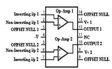
The 747 is a general purpose dual operational amplifier containing two 741 op-amps. The two operational amplifiers have a common bias network and power supply leads. Otherwise, their operation is completely independent. The characteristics of the op-amp are no latch-up when input common mode range is exceeded, freedom from oscillations. It is a 14-pin dual in line package (DIP), shown in figure below:

Pin Description of 747 Op-amp:

747 op-amp
Pin1 - Inverting input terminal of op-amp1
Pin2 - Non-inverting input terminal of op-amp1
Pin3 - Offset null terminal op-amp1
Pin4 - Negative supply voltage (-V)
Pin5 – Offset null terminal of op-amp2
Pin6 – Non-inverting input terminal of op-amp2
Pin7 – Inverting input terminal of op-amp2
Pin8 - Offset null terminal of op-amp2
Pin9 – Positive supply voltage (+V) of op-amp2
Pin10 – Output of op-amp2
Pin11 – No connection (NC)
Pin13 – Positive supply voltage of op-amp1
Pin14 – Offset null terminal of op-amp1

Features of 747 op-amp:

  • Dual supply voltage ±1.5V to ±15V
  • No frequency compensation required
  • Short-circuit protection
  • Wide common-mode and differential voltage ranges
  • Low power consumption
  • Unity gain stable
  • No latch-up
  • Balanced offset null
  • Supply current is less than 300 μA per amplifier at 5 V

How to test an Op Amp IC?

Operational Amplifiers are widely used in electronic circuits as amplifiers, comparators, voltage follower, summing amplifier etc. Most of the commonly used Op Amps like 741, TL071, CA3130, CA3140 etc have same pin configurations. Hence this tester is useful to check the working of the Op Amp during trouble shooting or servicing. It is an easy to make tool which is essential in the work bench of a hobbyist or technician.
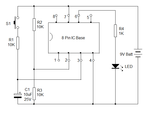
The tester is wired around an 8 pin IC base into which the IC to be tested can be inserted. Pin 2 (inverting input of IC) is connected to a potential divider R2, R3 that gives half supply voltage to pin 2. Pin 3 (None inverting input) of IC base is connected to the VCC through R1 and a Push to on switch. Output pin 6 is used to connect the visual indicator LED via the current limiting resistor R4.
OP-AMP-TESTER
The design is a voltage comparator. Insert the IC in to the socket with correct orientation. The notch at the left side of the IC should match with the notch in the IC base. In this comparator mode, the output of IC1 goes high when its pin 3 gets a higher voltage than pin 2. Here pin 2 gets 4.5 volts (if battery is 9V) and pin 3, 0 volts.
So the output remains low and LED will be dark. When S1 is pressed, pin 3 gets higher voltage than pin 2 and the output of IC turns high to light the LED. This indicates that the circuitry inside the IC is working.

Wednesday 4 March 2015

Different Motor Driving ICs used in Robots and different Mechanical Instruments

L9805E Super smart power motor driver with 8-Bit MCU, RAM, EEPROM, ADC, WDG, Timers, PWM and H-bridge driver

  • activeActive
The L9805 is a Super Smart Power device suited to drive resistive and inductive loads under software control. It includes a ST7 microcontroller and some peripherals. The microcontroller can execute the software contained in the program EPROM/ROM and drive, through dedicated registers, the power bridge.
The internal voltage regulators rated to the automotive environment, PWM modules, CAN transceiver and controller, ISO 9141 transceiver, timers, temperature sensor and the AtoD converter allow the device to realize by itself a complete application, in line with the most common mechatronic requirements.

Key Features

  • 6.4-18V Supply Operating Range
  • 16 MHz Maximum Oscillator Frequency
  • 8 MHz Maximum Internal Clock Frequency
  • Oscillator Supervisor
  • Fully Static operation
  • -40˚C to + 150˚C Temperature Range
  • User EPROM/OTP: 16 Kbytes
  • Data RAM: 256 bytes
  • Data EEPROM: 128 bytes
  • 64 pin HiQUAD64 package
  • 10 multifunctional bidirectional I/O lines
  • Two 16-bit Timers, each featuring: 2 Input Captures 2 Output Compares External Clock input (on Timer 1) PWM and Pulse Generator modes
  • Two Programmable 16-bit PWM generator modules.
  • CAN peripheral including Bus line interface according 2A/B passive specifications
  • 10-bit Analog-to-Digital Converter
  • Software Watchdog for system integrity
  • Master Reset, Power-On Reset, Low Voltage Reset
  • 70mΩ DMOS H-bridge.
  • 8-bit Data Manipulation
  • 63 basic Instructions and 17 main Addressing Modes
  • 8 x 8 Unsigned Multiply Instruction
  • True Bit Manipulation
  • Complete Development Support on DOS/WINDOWSTM™ Real-Time Emulator
  • Full Software Package on DOS/WINDOWSTM™ (C-Compiler, Cross-Assembler, Debugger)

L9903

ISO9141 Motor Bridge Controller
  • Active
Control circuit for power MOS bridge driver in automotive applications with ISO 9141bus interface.

Key Features

  • OPERATING SUPPLY VOLTAGE 8V TO 20V, OVERVOLTAGE MAX. 40V
  • OPERATING SUPPLY VOLTAGE 6V WITH IMPLEMENTED STEPUP CONVERTER
  • QUIESCENT CURRENT IN STANDBY MODE LESS THAN 50μA
  • ISO 9141 COMPATIBLE INTERFACE
  • CHARGE PUMP FOR DRIVING A POWER MOS AS REVERSE BATTERY PROTECTION
  • PWM OPERATION FREQUENCY UP TO 30KHZ
  • PROGRAMMABLE CROSS CONDUCTION PROTECTION TIME
  • OVERVOLTAGE, UNDERVOLTAGE, SHORT CIRCUIT AND THERMAL PROTECTION
  • REAL TIME DIAGNOSTIC

Circuit Diagram


L9904

Motor bridge Controller
  • Active
Control circuit for power MOS bridge driver in automotive applications with ISO 9141bus interface.

Key Features

  • OPERATING SUPPLY VOLTAGE 8V TO 28V, OVERVOLTAGE MAX. 40V
  • OPERATING SUPPLY VOLTAGE 6V WITH IMPLEMENTED STEPUP CONVERTER
  • QUIESCENT CURRENT IN STANDBY MODE LESS THAN 50μA
  • ISO 9141 COMPATIBLE INTERFACE
  • CHARGE PUMP FOR DRIVING A POWER MOS AS REVERSE BATTERY PROTECTION
  • PWM OPERATION FREQUENCY UP TO 30KHZ
  • PROGRAMMABLE CROSS CONDUCTION PROTECTION TIME
  • OVERVOLTAGE, UNDERVOLTAGE, SHORT CIRCUIT AND THERMAL PROTECTION
  • REAL TIME DIAGNOSTIC

Circuit Diagram


L9930

Dual Full Bridge
  • activeActive
The L9930 is a dual full-bridge. The output stages are Power Mos switches

Key Features

  • RDS ON = 2
  • INTERNAL CLAMPING VOLTAGE = 32V
  • INTERNAL FREE WHEELING DIODES
  • PARALLEL DRIVE CAPABILITY
  • RESISTIVE OR INDUCTIVE LOAD
  • PROTECTION:TEMPERATURE PROTECTIONSHORT-CIRCUIT PROTECTION (Vbat, LOAD, GND)
  • DETECTION:SHORTED LOADOPEN LOADOVERTEMPERATURE

Circuit Diagram


L9935

Two-Phase Stepper Motor Driver
  • activeActive
The L9935 is a two-phase stepper motor driver circuit suited to drive bipolar stepper motors.
The device can be controlled by a serial interface (SPI). All protections required to design a well protected system (short-circuit, over temperature, cross conduction etc.) are integrated

Key Features

  • 2 x 1.1 A full bridge outputs
  • Integrated chopping current regulation
  • Minimized power dissipation during flyback
  • Output stages with controlled output voltage slopes to reduce electromagnetic radiation
  • Short-circuit protection of all outputs
  • Error-flag for over load, open load and over temperature pre alarm
  • Delayed channel switch on to reduce peak currents
  • Max. operating supply voltage 24 V
  • Standby consumption typically 40 μA
  • Serial interface (SPI)

Circuit Diagram


L9942

Stepper Motor Driver for Bipolar Motors with microstepping & programmable current profile
  • activeActive
The L9942 is an integrated stepper motor driver for bipolar stepper motors with microstepping and programmable current profile look-up-table to allow a flexible adaptation of the stepper motor characteristics and intended operating conditions. It is possible to use different current profiles depending on target criteria: audible noise, vibrations, rotation speed or torque. The decay mode used in PWM-current control circuit can be programmed to slow-, fast-, mixed-and auto-decay. In auto decay mode device will use slow decay mode if the current for the next step will increase and the fast decay or mixed decay mode if the current will decrease. The programmable stall detection is useful in case of head lamp leveling and bending light application, by preventing to run the motor too long time in stall for position alignment. If a stall is detected, the alignment process is closed and the noise is minimized.

Key Features

  • Two full bridges for max. 1.3 A load(RDSON= 500 mΩ)
  • Programmable current waveform with look-up table: 9 entries with 5 bit resolution
  • Current regulation by integrated PWM controller and internal current sensing
  • Programmable stepping mode: full, half, mini and microstepping
  • Programmable slew rate for EMC and power dissipation optimization
  • Programmable Fast-, Slow-, Mixed- and Auto-Decay Mode
  • Full-scale current programmable with 3 bit resolution
  • Programmable stall detection
  • Step clock input for reduced μController requirements
  • Very low current consumption in standby mode IS< 3 μA, typ. Tj≤ 85 °C
  • All outputs short circuit protected with openload, overload current, temperature warning and thermal shutdown
  • The PWM signal of the internal PWM controller is available as digital output.
  • All parameters are guaranteed for 3 V < Vcc < 5.3 V and for 7 V < Vs < 20 V

Circuit Diagram


L9958

SPI Controlled H-Bridge
  • Active
The L9958 is an SPI controlled H-Bridge, designed for the control of DC and stepper motors in safety critical applications and under extreme environmental conditions.
The H-Bridge is protected against over temperature, short circuits and has an undervoltage lockout for all the supply voltages Vsand Vdd, and for overvoltage on Vdd. All malfunctions cause the output stages to go tristate.
Detailed failure diagnostics on each channel is provided via SPI: short circuit to battery, short circuit to ground, short circuit overload, over temperature.
Open-load can be detected in ON condition, for the widest application ranges. Current regulation threshold can be set by SPI from 2.5 A to 8.6 A (Typ.), in 4 steps. Guaranteed accuracy is ±10 % on all temp range, using an external reference resistor with 1% accuracy over all temp range.
Current limitation threshold is linearly reduced by temperature over 165 °C.and a thermal warning bit is set by SPI. The H-Bridge contains integrated free-wheel diodes. In case of free-wheeling condition, the low side transistor is switched on in parallel of its diode to reduce power dissipation.
A multiple wire bonding technique, as well as ST proprietary package design is making L9958 compatible with three power packages, for maximum flexibility:
PowerSO-20 package (medium power, JEDEC standard MO166);PowerSO16 package (medium power, lower cost);PowerSSO24 package (low power, very low cost JEDEC standard MO271A).

Key Features

  • Programmable current regulation peak threshold by SPI up to 8.6 A typ.
  • Operating battery supply voltage 4.0 V to 28 V
  • Operating Vdd supply voltage 4.5 V to 5.5 V
  • All pins withstand 19 V, Vs and output pins withstand 40 V
  • Full path Ronfrom 100 mΩ (at T= -40 °C) to 300 mΩ (at Tj=150 °C)
  • Logic inputs TTL/CMOS-compatible
  • Operating frequency up to 20 kHz
  • 16-bit SPI interface for configuration/diagnostics, daisy chain capability
  • Over temperature and short circuit protection
  • VSundervoltage disable function
  • Vddundervoltage and overvoltage protection
  • Vddovervoltage detection
  • Open-load detection in ON condition
  • Full diagnostics in OFF state
  • Enable and disable input
  • Low stand by current (<10 μA)
  • Voltage and current slew-rate control for low EMI, programmable through SPI
  • Available in three power packages

Circuit Diagram


L9959T

Dual DC motor driver
  • Active
L9959S and L9959T are a single and dual integrated H-bridges for resistive and inductive loads featuring output current direction and supervising functions.
The PowerSSO24 houses one full H-Bridge, while the PowerSSO36 houses two H-Bridges that can work in parallel, through independent input driving commands.
Target application ranges from throttle control actuators to exhaust gas recirculation control valves in automotive domain to a more general use to drive DC and Stepper motors.

Key Features

  • Full path RDSONless than 540 mΩ
  • Continuous load current > 3 A
  • Operating battery supply voltage 5 V to 28 V
  • Operating VDD supply voltage 4.5 V to 5.5 V
  • All ECU internal pins can withstand up to 18 V
  • Output switching frequency up to 11 kHz
  • Monitoring of VDD supply voltage
  • SPI programmable output current limitation from 5 A to 8.6 A (in 3 steps)
  • Over temperature and short circuit protection
  • Full diagnosis capability
  • Fast switch-off open-drain input/output
  • Current-monitoring with current feedback output signal CF
  • SPI-interface for configuration and diagnosis
  • Error history in second diagnosis register
  • Two independent enable pins: "/ABE" and "DIS"
  • Control of power stages by SPI or two input signals, PWM and DIR (configurable via SPI)
  • Logic levels 5 V compatible
  • Conformity to improved EMC requirements due to smart H-bridge switching

L9997ND

Dual Half Bridge Driver
  • activeActive
The L9997ND is a monolithic integrated driver, in BCD technology intended to drive various loads,including DC motors. The circuit is optimized for automotive electronics environmental conditions.

Key Features

  • HALF BRIDGE OUTPUTS WITH TYPICAL RON = 0.7
  • OUTPUT CURRENT CAPABILITY ±1.2A
  • OPERATING SUPPLY VOLTAGE RANGE 7V TO 16.5V
  • SUPPLY OVERVOLTAGE PROTECTION FUNCTION FOR VVS UP TO 40V
  • VERY LOW QUIESCENT CURRENT IN STANDBY MODE < 1µA
  • CMOS COMPATIBLE INPUTS WITH HYSTERESIS
  • OUTPUT SHORT-CIRCUIT PROTECTION
  • THERMAL SHUTDOWN
  • REAL TIME DIAGNOSTIC: THERMAL OVERLOAD, OVERVOLTAGE

Circuit Diagram


L99ASC03

Brushless/Sensorless 3-phase motor pre-driver for automotive applications
  • Active
The L99ASC03 is a multifunctional system IC designed for three-phase motor control applications.
The device features a voltage regulator to supply an external microcontroller and an operation amplifier for motor current sensing. It is designed to control six externalN-channel MOSFETs in bridge configuration to drive three-phase motors in automotive applications. All gate driver outputs are controlled by separate inputs.
The integrated Serial Peripheral Interface (SPI) makes it possible to adjust device parameters, control all operating modes and read out diagnostic information.

Key Features

  • Automotive qualified
  • 5 V low-drop voltage regulator (200 mA continuous mode)
  • Very low current consumption in standby mode (typ. 15 μA)
  • ST SPI interface for control and diagnostics
  • Window watchdog and fail-safe functionality
  • Two separate power supply pins
  • Three half-bridge drivers to control external MOSFETs (configurable by SPI)
  • Full drive of external MOSFETs down to 6 V input voltage
  • Input pin for each gate driver (with cross-current protection)
  • Two-stage charge pump supporting 100% duty cycle
  • PWM operation up to 80 kHz (not restricted)
  • Current-sense amplifier (configurable by SPI)
  • Disable input to turn off gate driver outputs
  • Analog multiplexer output to monitor external power supply voltages and internal junction temperature
  • Advanced BEMF detection IP
  • Overcurrent protection (programmable)
  • Drain-source monitoring and open-load detection
  • TQFP48 7 x 7 x 1 mm with Exposed Pad (4.5 x 4.5 mm) package

L99H01

Motor bridge driver for automotive applications
  • Active
The L99H01 is designed to control 4 external N-channel MOS transistors in bridge configuration for DC-motor driving in automotive applications. A free configurable current sense amplifier is integrated. The integrated standard serial peripheral interface (SPI) controls all outputs and provides diagnostic information. An interface pin for the thermal sensors of the external MOSFETs is implemented.

Key Features

  • Operating supply voltage 6 V to 28 V
  • Central 2 stage charge pump
  • 100% duty cycle
  • Full RDSon down to 6 V (normal level MOSFETs)
  • Control of reverse battery protection MOSFET
  • Charge pump current limited
  • PWM operation up to 30 kHz
  • SPI interface
  • Current sense amplifier / free configurable
  • Zero adjust for end of line trimming
  • Power management: programmable free wheeling
  • Sensing circuitry of external MOSFETs with embedded thermal sensors

Circuit Diagram


L99MD01

Standard Functions, Motor Drivers
  • Active
The L99MD01 is an octal half-bridge driver for automotive applications.
The device is intended to drive DC and/or stepper motors. Using the boost converter it’s possible to drive 4 stepper motors simultaneously. Without boost converter the system is able to run 3 stepper motors in sequential mode or 2 stepper motors simultaneously. The octal half bridge configuration allows also to drive 4 DC-motors simultaneously and 7 DC-motors sequentially.
The integrated 24 bit standard Serial Peripheral Interface (SPI) controls all outputs and provides diagnostic information: normal operation, open-load in on-state, overcurrent, temperature warning and overtemperature.

Key Features

  • 8 half bridges
  • RON = typ. 0.9 Ω (HS), 0.64 Ω (LS) @ Tj= 25 °C
  • Current limit of each output at min. 0.8 A
  • Intrinsic DC/DC step up converter driving an external MOSFET
  • PWM mode option for all half bridges for hold current
  • Internal PWM generation
  • Two current monitor outputs
  • SPI interface for data communication
  • Temperature warning
  • All outputs over temperature protected
  • All outputs short circuit protected
  • VCC supply voltage 3.0 to 5.3 V
  • Very low current consumption in standby mode typ. 5 μA
  • Voperating range compliant: 6 V – 18 V

L99MD02

Standard Functions, Motor Drivers
  • activeActive
The L99MD02 IC is a 6 x half bridge driver for automotive applications. The device is intended to drive DC-motors. It is possible to drive 3 DC-motors simultaneously or up to 5 DC-motors sequentially.
The integrated 24 bit standard serial peripheral interface (SPI) controls all outputs and provides diagnostic information: normal operation, open-load in on-state, overcurrent, temperature warning and overtemperature.

Key Features

  • 6 half bridges
  • RON= typ.0.9 Ω (HS), 0.64 Ω (LS) at Tj= 25 °C
  • Current limit of each output at minimum 0.8 A
  • Internal PWM generation
  • PWM mode option for all half bridges for hold current
  • Two current monitor outputs
  • SPI interface for data communication
  • Temperature warning
  • All outputs over temperature protected
  • All outputs short circuit protected
  • VCC supply voltage 3.0 to 5.3 V
  • Very low current consumption in standby mode typ. 5 μA
  • Voperating range compliant: 6 – 18 V

VN5770AKP-E

Quad smart power solid state relay for complete H-bridge configurations
  • Active
The VN5770AKP-E is a device formed by three monolithic chips housed in a standard SO-28 package: a double high-side and two low-side switches. The double high-side is made using STMicroelectronics®VIPower®M0-5 technology, while the low-side switches are fully protected VIPower M0-3 OMNIFET II. This device is suitable to drive a DC motor in a bridge configuration as well as to be used as a quad switch for any low voltage application.
The dual high-side switches integrate built in non latching thermal shutdown with thermal hysteresis. An output current limiter protects the device in overload condition. In case of long overload duration, the device limits the dissipated power to a safe level up to thermal shutdown intervention. An analog current sense pin delivers a current proportional to the load current (according to a known ratio) and indicates overtemperature shutdown of the relevant high-side switch through a voltage flag.
The low-side switches have built in non latching thermal shutdown with thermal hysteresis, linear current limitation and overvoltage clamping.
Fault feedback for overtemperature shutdown of the low-side switch is indicated by the relevant input pin current consumption going up to the fault sink current flag.

Key Features

  • ECOPACK®: lead free and RoHS compliant
  • Automotive Grade: compliance with AEC guidelines
  • General features
  • Inrush current management by active power limitation on the high-side switches
  • Very low standby current
  • Very low electromagnetic susceptibility
  • Compliance with European directive 2002/95/EC
  • Protection
  • High-side drivers undervoltage shutdown
  • Overvoltage clamp
  • Output current limitation
  • High and low-side overtemperature shutdown
  • Short circuit protection
  • ESD protection
  • Diagnostic functions
  • Proportional load current sense
  • Thermal shutdown indication on both the high and low-side switches

VN5772AK-E

Quad smart power solid state relay for complete H bridge configurations
  • Active
The VN5772AK-E is a device formed by three monolithic chips housed in a standard SO-28 package: a double high-side and two low-side switches. The double high-side is made using STMicroelectronics®VIPower®M0-5 technology, while the low-side switches are fully protected VIPower M0-5 OMNIFET III. This device is suitable to drive a DC motor in a bridge configuration as well as to be used as a quad switch for any low-voltage application. The dual high-side switches integrate built-in non latching thermal shutdown with thermal hysteresis. An output current limiter protects the device in overload conditions. In the case of long overload duration, the device limits the dissipated power to a safe level-up to thermal shutdown intervention. An analog current sense pin delivers a current proportional to the load current (according to a known ratio) and indicates overtemperature shutdown of the relevant high-side switch through a voltage flag.The low-side switches have built-in non latching thermal shutdown with thermal hysteresis, linear current limitation and overvoltage clamping. In case of long overload duration, the low-side switches limit the dissipated power to a safe level up to the thermal shutdown intervention. Fault feedback for overtemperature shutdown of the low-side switch is indicated by the relevant status pin.

Key Features

  • General features
  • Inrush current management by active power limitation on the high-side switches
  • Very low standby current
  • Very low electromagnetic susceptibility
  • Compliant with European directive 2002/95/EC
  • Protections
  • High-side drivers under voltage shutdown
  • Overvoltage clamp
  • Output current limitation
  • High and low-side overtemperature shutdown
  • Short-circuit protection
  • ESD protection
  • Diagnostic functions
  • Proportional load current sense
  • Thermal shutdown indication on both the high and low-side switches

Circuit Diagram


VN770KP-E

Quad smart power solid state relay for complete H-bridge configurations
  • Active
The VN770KP-E is a device formed by three monolithic chips housed in a standard SO-28 package: a double high side and two low side switches. Both the double high side and low side switches are made using STMicroelectronics VIPower™ M0-3 Technology.
This device is suitable to drive a DC motor in a bridge configuration as well as to be used as a quad switch for any low voltage application.
The dual high side switches have built-in thermal shutdown to protect the chips from over temperature and current limiter blocks to protect the device from short circuit. Status output is provided to indicate open load in off and on-state and over temperature.
The low side switches are two OMNIFET II types (fully auto protected Power MOSFET in VIPower™ technology). They have built-in thermal shutdown, linear current limitation and overvoltage clamping. Fault feedback for thermal intervention can be detected by monitoring the voltage at the input pin.

Key Features

  • ECOPACK®: lead free and RoHS compliant
  • Automotive Grade: compliance with AEC guidelines
  • Suited as low voltage bridge
  • Linear current limitation
  • Very low standby power dissipation
  • Short circuit protected
  • Status flag diagnostic (open drain)
  • Integrated clamping circuits
  • Undervoltage protection
  • ESD protection

VN771KP-E

Quad smart power solid state relay for complete H-bridge configurations
  • activeActive
The VN771KP-E is a device formed by three monolithic chips housed in a standard SO-28 package: a double high side and two low side switches. Both the double high side and low side switches are made using STMicroelectronics VIPowerM0-3 Technology.
This device is suitable to drive a DC motor in a bridge configuration as well as to be used as a quad switch for any low voltage application.
The dual high side switches have built-in thermal shutdown to protect the chips from over temperature and current limiter blocks to protect the device from short circuit. Status output is provided to indicate open load in off and on-state and over temperature.
The low side switches are two OMNIFET II types (fully auto protected Power MOSFET in VIPowertechnology). They have built-in thermal shutdown, linear current limitation and overvoltage clamping. Fault feedback for thermal intervention can be detected by monitoring the voltage at the input pin.

Key Features

  • ECOPACK®: lead free and RoHS compliant
  • Automotive Grade: compliance with AEC guidelines
  • Suited as low voltage bridge
  • Linear current limitation
  • Very low standby power dissipation
  • Short circuit protected
  • Status flag diagnostic (open drain)
  • Integrated clamping circuits
  • Undervoltage protection
  • ESD protection

VN772KP-E

Quad smart power solid state relay for complete H-bridge configurations
  • Active
The VN772KP-E is a device formed by three monolithic chips housed in a standard SO-28 package: a double high side and two low side switches. Both the double high side and low side switches are made using STMicroelectronics VIPower™ M0-3 Technology.
This device is suitable to drive a DC motor in a bridge configuration as well as to be used as a quad switch for any low voltage application.
The dual high side switches have built-in thermal shutdown to protect the chips from over temperature and current limiter blocks to protect the device from short circuit. Status output is provided to indicate open load in off and on-state and over temperature.
The low side switches are two OMNIFET II types (fully auto protected Power MOSFET in VIPower™ technology). They have built-in thermal shutdown, linear current limitation and overvoltage clamping. Fault feedback for thermal intervention can be detected by monitoring the voltage at the input pin.

Key Features

  • ECOPACK®: lead free and RoHS compliant
  • Automotive Grade: compliance with AEC guidelines
  • Suited as low voltage bridge
  • Linear current limitation
  • Very low standby power dissipation
  • Short circuit protected
  • Status flag diagnostic (open drain)
  • Integrated clamping circuits
  • Undervoltage protection
  • ESD protection

VNH2SP30-E

AUTOMOTIVE FULLY INTEGRATED H-BRIDGE MOTOR DRIVER
  • Active
The VNH2SP30-E is a full bridge motor driver intended for a wide range of automotive applications. The device incorporates a dual monolithic high side driver and two low side switches. The high side driver switch is designed using STMicroelectronic’s well known and proven proprietary VIPower™ M0 technology which permits efficient integration on the same die of a true Power MOSFET with an intelligent signal/protection circuitry.
The low side switches are vertical MOSFETs manufactured using STMicroelectronic’s proprietary EHD (`STripFET™’) process. The three die are assembled in the MultiPowerSO-30 package on electrically isolated leadframes. This package, specifically designed for the harsh automotive environment offers improved thermal performance thanks to exposed die pads.
Moreover, its fully symmetrical mechanical design allows superior manufacturability at board level.
The input signals INA and INB can directly interface to the microcontroller to select the motor direction and the brake condition. The DIAGA/ENA or DIAGB/ENB, when connected to an external pull-up resistor, enable one leg of the bridge. They also provide a feedback digital diagnostic signal. The normal condition operation is explained in Table 12: Truth table in normal operating conditions on page 14. The motor current can be monitored with the CS pin by delivering a current proportional to its value. The speed of the motor can be controlled in all possible conditions by the PWM up to 20 kHz. In all cases, a low level state on the PWM pin will turn off both the LSA and LSB switches. When PWM rises to a high level, LSA or LSB turn on again depending on the input pin state.

Key Features

  • 5V logic level compatible inputs
  • Undervoltage and overvoltage shut-down
  • Overvoltage clamp
  • Thermal shut down
  • Cross-conduction protection
  • Linear current limiter
  • Very low stand-by power consumption
  • PWM operation up to 20 kHz
  • Protection against loss of ground and loss of VCC
  • Current sense output proportional to motor current
  • Package: ECOPACK®

Circuit Diagram


VNH3ASP30-E

AUTOMOTIVE FULLY INTEGRATED H-BRIDGE MOTOR DRIVER
  • activeActive
The VNH3ASP30-E is a full-bridge motor driver intended for a wide range of automotive applications. The device incorporates a dual monolithic high-side driver (HSD) and two lowside switches. The HSD switch is designed using STMicroelectronics proprietary VIPower™ M0 technology that efficiently integrates a true Power MOSFET with an intelligent signal/protection circuit on the same die.
The low-side switches are vertical MOSFETs manufactured using STMicroelectronics proprietary EHD ("STripFET™") process.The three circuits are assembled in a MultiPowerSO- 30 package on electrically isolated lead frames.
This package, specifically designed for the harsh automotive environment, offers improved thermal performance thanks to exposed die pads.
Moreover, its fully symmetrical mechanical design provides superior manufacturability at board level.
The input signals INA and INB can directly interface with the microcontroller to select the motor direction and the brake condition. Pins DIAGA/ENA or DIAGB/ENB, when connected to an external pull-up resistor, enable one leg of the bridge. They also provide a feedback digital diagnostic signal. The CS pin monitors the motor current by delivering a current proportional to its value. The speed of the motor can be controlled in all possible conditions by the PWM up to 20 kHz. In all cases, a low level state on the PWM pin will turn off both the LSA and LSB switches. When PWM rises to a high level, LSA or LSB turn on again depending on the input pin state.

Key Features

  • 5V logic level compatible inputs
  • Undervoltage and overvoltage shutdown
  • Overvoltage clamp
  • Thermal shut down
  • Cross-conduction protection
  • Linear current limiter
  • Very low standby power consumption
  • PWM operation up to 20 kHz
  • Protection against loss of ground and loss of VCC
  • Current-sense output proportional to motor current
  • Package: ECOPACK®

Circuit Diagram


VNH3SP30-E

AUTOMOTIVE FULLY INTEGRATED H-BRIDGE MOTOR DRIVER
  • activeActive
The VNH3SP30-E is a full-bridge motor driver intended for a wide range of automotive applications. The device incorporates a dual monolithic high-side driver (HSD) and two low-side switches. The HSD switch is designed using STMicroelectronics proprietary VIPower™ M0-3 technology that efficiently integrates a true Power MOSFET with an intelligent signal/protection circuit on the same die.
The low-side switches are vertical MOSFETs manufactured using STMicroelectronics proprietary EHD (“STripFET™”) process.The three circuits are assembled in a MultiPowerSO-30 package on electrically isolated lead frames. This package, specifically designed for the harsh automotive environment, offers improved thermal performance thanks to exposed die pads. Moreover, its fully symmetrical mechanical design provides superior manufacturability at board level. The input signals INA and INB can directly interface with the microcontroller to select the motor direction and the brake condition. Pins DIAGA/ENA or DIAGB /ENB, when connected to an external pull-up resistor, enable one leg of the bridge. They also provide a feedback digital diagnostic signal. The normal condition operation is explained in The speed of the motor can be controlled in all possible conditions by the PWM up to kHz. In all cases, a low level state on the PWM pin will turn off both the LSAand LSB switches. When PWM rises to a high level, LSA or LSB turn on again depending on the input pin state.

Key Features

  • Output current: 30A
  • 5V logic level compatible inputs
  • Undervoltage and overvoltage shutdown
  • Overvoltage clamp
  • Thermal shut down
  • Cross-conduction protection
  • Linear current limiter
  • Very low standby power consumption
  • PWM operation up to 10 kHz
  • Protection against loss of ground and loss of VCC
  • Package: ECOPACK®

Circuit Diagram


VNH5019A-E

Automotive fully integrated H-bridge motor driver
  • activeActive
The VHN5019A-E is a full bridge motor driver intended for a wide range of automotive applications. The device incorporates a dual monolithic high-side drivers and two low-side switches. The high-side driver switch is designed using STMicroelectronics’ well known and proven proprietary VIPower®M0 technology that allows to efficiently integrate on the same die a true Power MOSFET with an intelligent signal/protection circuit.
The three dice are assembled in MultiPowerSO-30 package on electrically isolated lead-frames. This package, specifically designed for the harsh automotive environment offers improved thermal performance thanks to exposed die pads. The input signals INAand INBcan directly interface to the microcontroller to select the motor direction and the brake condition.
The DIAGA/ENAor DIAGB/ENB, when connected to an external pull-up resistor, enable one leg of the bridge. They also provide a feedback digital diagnostic signal. The CS pin allows to monitor the motor current by delivering a current proportional to its value when CS_DIS pin is driven low or left open. The PWM, up to 20 KHz, lets us to control the speed of the motor in all possible conditions. In all cases, a low-level state on the PWM pin turns-off both the LSAand LSBswitches. When PWM rises to a high-level, LSAor LSBturn-on again depending on the input pin state.
Output current limitation and thermal shutdown protects the concerned high-side in short to ground condition.
The short to battery condition is revealed by the overload detector or by thermal shutdown that latches off the relevant low-side.
Active VCCpin voltage clamp protects the device against low energy spikes in all configurations for the motor.
CP pin provides the necessary gate drive for an external n-channel PowerMOS used for reverse polarity protection.

Key Features

  • ECOPACK®: lead free and RoHS compliant
  • Automotive Grade: compliance with AEC guidelines
  • Output current: 30 A
  • 3 V CMOS compatible inputs
  • Undervoltage and overvoltage shutdown
  • High-side and low-side thermal shutdown
  • Cross-conduction protection
  • Current limitation
  • Very low standby power consumption
  • PWM operation up to 20 khz
  • Protection against:
  • Loss of ground and loss of VCC
  • Current sense output proportional to motor current
  • Charge pump output for reverse polarity protection
  • Output protected against short to ground and short to VCC

Circuit Diagram


VNH5050A-E

Automotive fully integrated H-bridge motor driver
  • activeActive
The VNH5050A-E is a full bridge motor driver intended for a wide range of automotive applications. The device incorporates a dual monolithic high-side driver and two low-side switches. All switches are designed using STMicroelectronics®well known and proven proprietary VIPower®M0 technology that allows to efficiently integrate on the same die a true Power MOSFET with an intelligent signal/protection circuitry. The three dies are assembled in a PowerSSO-36 TP package on electrically isolated lead frames. This package, specifically designed for the harsh automotive environment offers improved thermal performance thanks to exposed die pads. Moreover, its fully symmetrical mechanical design allows superior manufacturability at board level. The input signals INAand INBcan directly interface to the microcontroller to select the motor direction and the brake condition. The DIAGA/ENAor DIAGB/ENB, when connected to an external pull-up resistor, enables one leg of the bridge. Each DIAGA/ENAprovides a digital diagnostic feedback signal as well. The normal operating condition is explained in the truth table. The CS pin allows monitoring the motor current by delivering a current proportional to its value when CS_DIS pin is driven low or left open. When CS_DIS is driven high, CS pin is in high impedance condition. The PWM, up to 20 KHz, allows to control the speed of the motor in all possible conditions. In all cases, a low level state on the PWM pin turns off both the LSAand LSBswitches.

Key Features

  • Output current: 30 A
  • 3 V CMOS compatible inputs
  • Undervoltage and overvoltage shutdown
  • Overvoltage clamp
  • Thermal shutdown
  • Cross-conduction protection
  • Current and power limitation
  • Very low standby power consumption
  • PWM operation up to 20 KHz
  • Protection against loss of ground and loss of VCC
  • Current sense output proportional to motor current
  • Output protected against short to ground and short to VCC
  • Package: ECOPACK®

Circuit Diagram


VNH5180A-E

Automotive fully integrated H-bridge motor driver
  • Active
The VNH5180A-E is a full bridge motor driver intended for a wide range of automotive applications. The device incorporates a dual monolithic high-side driver and two low-side switches. Both switches are designed using STMicroelectronics’ well known and proven proprietary VIPower®M0 technology that allows to efficiently integrate on the same die a true Power MOSFET with an intelligent signal/protection circuitry. The three dies are assembled in PowerSSO-36 TP package on electrically isolated leadframes. This package, specifically designed for the harsh automotive environment offers improved thermal performance thanks to exposed die pads. Moreover, its fully symmetrical mechanical design allows superior manufacturability at board level. The input signals INAand INBcan directly interface to the microcontroller to select the motor direction and the brake condition. The DIAGA/ENAor DIAGB/ENB, when connected to an external pull-up resistor, enables one leg of the bridge. Each DIAGA/ENAprovides a feedback digital diagnostic signal as well. The normal operating condition is explained in the truth table. The CS pin allows to monitor the motor current by delivering a current proportional to its value when CS_DIS pin is driven low or left open. When CS_DIS is driven high, CS pin is in high impedance condition. The PWM, up to 20 KHz, allows to control the speed of the motor in all possible conditions. In all cases, a low level state on the PWM pin turns off both the LSAand LSBswitches.

Key Features

  • Output current: 8 A
  • 3 V CMOS compatible inputs
  • Undervoltage shutdown
  • Overvoltage clamp
  • Thermal shutdown
  • Cross-conduction protection
  • Current and power limitation
  • Very low standby power consumption
  • PWM operation up to 20 KHz
  • Protection against loss of ground and loss of VCC
  • Current sense output proportional to motor current
  • Output protected against short to ground and short to VCC
  • Package: ECOPACK®

Circuit Diagram

VNH5200AS-E

Automotive fully integrated H-bridge motor driver
  • PreviewPreview
The VNH5200AS-E is a full bridge motor driver intended for a wide range of automotive applications. The device incorporates a dual monolithic high-side driver and two low-side switches.
Both switches are designed using STMicroelectronics’ well known and proven proprietary VIPower®M0 technology that allows to efficiently integrate on the same die a true Power MOSFET with an intelligent signal/protection circuitry. The three dies are assembled in SO-16N package on electrically isolated leadframes. Moreover, its fully symmetrical mechanical design allows superior manufacturability at board level. The input signals INAand INBcan directly interface to the microcontroller to select the motor direction and the brake condition. The DIAGA/ENAor DIAGB/ENB, when connected to an external pull-up resistor, enables one leg of the bridge. Each DIAGA/ENAprovides a feedback digital diagnostic signal as well. The normal operating condition is explained in the truth table. The CS pin allows to monitor the motor current by delivering a current proportional to its value.

Key Features

  • Automotive qualified
  • Output current: 8 A
  • 3 V CMOS-compatible inputs
  • Undervoltage shutdown
  • Overvoltage clamp
  • Thermal shutdown
  • Cross-conduction protection
  • Current and power limitation
  • Very low standby power consumption
  • Protection against loss of ground and loss of VCC
  • Current sense output proportional to motor current
  • Output protected against short to ground and short to VCC
  • Package: ECOPACK®

VNH7013XP-E

Automotive integrated H-bridge
  • activeActive
The VNH7013XP-E is an automotive integrated H-bridge intended for a wide range of automotive applications driving DC motors. The device incorporates a dual channel and two single channel MOSFETs. All the devices are designed using STMicroelectronics®well known and proven proprietary VIPower®M0-S7 technology that allows to integrate in a package four different channels in H-bridge topology.
This package, specifically designed for the harsh automotive environment offers improved thermal performance thanks to exposed die pads. Moreover, its fully symmetrical mechanical design allows superior manufacturability at board level.

Key Features

  • Maximum VCCvoltage: 72 V
  • 10 V compatible inputs
  • RDS(on)per leg: 13 mΩ typical
  • Embedded thermal sensor: -8.1 mV/°K
  • Very low stray inductance in power line

VNH7100AS-E

Automotive fully integrated H-bridge motor driver
  • Preview
The VNH7070AS-E is a full bridge motor driver intended for a wide range of automotive applications. The device incorporates a dual monolithic high-side driver and two low-side switches.
Both switches are designed using STMicroelectronics’ well known and proven proprietary VIPower®M0 technology that allows to efficiently integrate on the same die a true Power MOSFET with an intelligent signal/protection circuitry. The three dies are assembled in SO-16N package on electrically isolated leadframes.
Moreover, its fully symmetrical mechanical design allows superior manufacturability at board level. The input signals INAand INBcan directly interface to the microcontroller to select the motor direction and the brake condition. A SEL0 pin is available to address to the microcontroller the information available on the MultiSense. The MultiSense pin allows to monitor the motor current by delivering a current proportional to the motor current value. The normal operating condition is explained in the truth table.
The PWM, up to 20 KHz, allows to control the speed of the motor in all possible conditions. In all cases, a low level state on the PWM pin turns off both the LSAand LSBswitches.

Key Features

  • Output current: 15 A
  • 3 V CMOS-compatible inputs
  • Undervoltage shutdown
  • Overvoltage clamp
  • Thermal shutdown
  • Cross-conduction protection
  • Current and power limitation
  • Very low standby power consumption
  • Protection against loss of ground and loss of VCC
  • PWM operation up to 20 KHz
  • MultiSense diagnostic functions
  • Analog motor current feedback
  • Output short to ground detection
  • Thermal shutdown indication
  • OFF-state open-load detection
  • Output short to VCCdetection
  • Output protected against short to ground and short to VCC
  • Standby Mode
  • Half Bridge Operation
  • Package: ECOPACK®


Please do Comments for further improvements. Yet there are many more ICs which are used to drive Motors. All the above ICs are made by STMicroelectronics