IC 741
The most commonly used op-amp is IC741. The 741 op-amp is a voltage amplifier, it inverts the input voltage at the output, can be found almost everywhere in electronic circuits.
Pin Configuration:
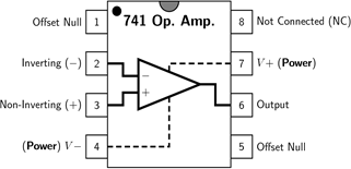
Let’s see the pin configuration and testing of 741 op-amps. Usually, this is a numbered counter clockwise around the chip. It is an 8 pin IC. They provide superior performance in integrator, summing amplifier and general feedback applications. These are high gain op-amp; the voltage on the inverting input can be maintained almost equal to Vin.
It is a 8-pin dual-in-line package with a pinout shown above.
Pin 1: Offset null.
Pin 2: Inverting input terminal.
Pin 3: Non-inverting input terminal.
Pin 4: –VCC (negative voltage supply).
Pin 5: Offset null.
Pin 6: Output voltage.
Pin 7: +VCC (positive voltage supply).
Pin 8: No Connection.
The main pins in the 741 op-amp are pin2, pin3 and pin6. In inverting amplifier, a positive voltage is applied to pin2 of the op-amp; we get output as negative voltage through pin 6. The polarity has been inverted. In a non-inverting amplifier, a positive voltage is applied to pin3 of the op-amp; we get output as positive voltage through pin 6. Polarity remains the same in non-inverting amplifier. Vcc is usually in the range from 12 to 15 volts. When two supplies (+Vcc/-Vcc) are used, they are the same voltage and of opposite sign in almost all cases. Remember that the operational amplifier is a high gain, differential voltage amplifier. For a 741 operational amplifier, the gain is at least 100,000 and can be more than a million (1,000,000). That’s an important fact you’ll need to remember as you put the 741 into a circuit.
There are many common application circuits using IC741 op-amp, they are adder, comparator, subtractor, integrator, differentiator and voltage follower.
Below is some example of 741 IC based circuits. However, the 741 is used as a comparator and not an amplifier. The difference between the two is small but significant. Even if used as a comparator the 741 still detects weak signals so that they can be recognized more easily. A comparator is a circuit that compares two input voltages. One voltage is called the reference voltage and the other is called the input voltage. It is a circuit which compares a signal voltage applied at one input of an op-amp with a known reference voltage at the other input. The 741 op-amp has ideal transfer characteristics (output ±Vsat); and the output is changed by increment in the input voltage of 2mV.
LM324
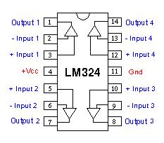
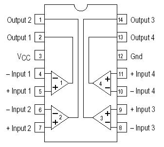
LM324 is a quad op amp integrated circuit with high stability, bandwidth which was designed to operate from a single power supply over a wide range of voltages. They have some dissimilar advantages over standard operational amplifier types in single supply applications. It is a 14-pin dual in-line package, contains four internally compensated and two stage operational amplifiers, shown in figure.
- Pin 1, 7, 8 and 14 are the outputs of comparator
- Pin 2, 6, 9 and 13 are the inverting inputs of compactor
- Pin 3, 5, 10 and 12 are non-inverting inputs of comparator
- Pin 11 is ground (0V)
- Pin 4 is supply voltage; 5V
Features:
Internally frequency compensated for unity gain
Large DC voltage gain 100 dB
Wide bandwidth 1 MHz
Wide power supply range: Single supply 3V to 32V
Essentially independent of supply voltage
Differential input voltage range equal to the power supply voltage
Large output voltage swing 0V to V+ − 1.5V
Potential dividers of LM323 are connected to the inverting and non inverting inputs of the op-amp to give some voltage at these terminals. Supply voltage is given to +V and –V is connected to ground. The output of this comparator will be logic high if the non-inverting terminal input is greater than the inverting terminal input of the comparator. When the inverting input is more than the non-inverting then logic low (0) will be the output.
Working of LM324:
When the power is applied to non-inverting terminal which is less than the inverting voltage of op-amp then the output becomes zero which means there is no current flow. Because we already know that when “+ > – = 1”. Here the ‘+ ‘sign indicates non-inverting terminal and ‘-‘sign indicates the inverting terminal.
If the non-inverting voltage is greater than the inverting voltage then the output will be high.
In this output of LM324 is internally connected to some resistance and it has some arrangement inside the IC, which makes a lot of difference to other comparators.
It is internally pulled-up, so no need of any resistor connection from the supply.
LM339
The LM339 is a most commonly used comparator, designed for use in level detection, low−level sensing and memory applications in automotive and industrial electronic applications. It has four inbuilt comparators; it compares two input voltage levels and gives digital output to show the bigger one.
These comparators additionally have a unique characteristic in that the input common-mode voltage range includes ground, in spite of the fact that they are operated from a single power supply voltage.
- Pin 1, 2, 13 and 14 are the outputs of comparator
- Pin 3 is supply voltage; 5V
- Pin 4, 6, 8 and 10 are inverting inputs of comparator
- Pin 5, 7, 9 and 11 are non-inverting inputs of comparator
- Pin 12 is ground; (0V)
Features:
- Signal or dual supply operation
- Wide operating supply range (VCC=2V~36V)
- Max Rating: 2 V to 36 V
- Tested to 30 V: Non-V Devices
- Input common-mode voltage includes ground
- Low supply current drain (IF=0.8mA)
- Open collector outputs for wired and connection
- Low input bias current 25nA
- Low output saturation voltage
- Output compatible with TTL, DTL, and CMOS logic system
- Differential input voltage range equal to the power supply voltage
Potential dividers of LM339 are connected to the inverting and non-inverting inputs of the op-amp to give some voltage at these terminals. Supply voltage is given to +V and –V is connected to ground. The output of this comparator will be logic high if the non-inverting terminal input is greater than the inverting terminal input of the comparator.
Working of LM339:
- When the power is applied to non-inverting terminal which is less than the inverting voltage of op-amp then the output becomes zero which means there is no current flow. Because we already know that when “+ > – = 1”. Here the ‘+ ‘sign indicates non-inverting terminal and ‘-‘sign indicates the inverting terminal.
- If the non-inverting voltage is greater than the inverting voltage then the current flow will be in the device.
- The LM339 is act as an open-collector that’s why we connected the resister from the supply, if we remove the resister then there is no current flow in the circuit.
LM358
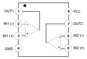
The LM358 op-amps are used in transducer amplifiers, dc gain blocks and all the conventional op-amp circuits which now can be more easily implemented in single power supply systems. For example, the LM358 op-amp can be directly operated off of the standard +5V power supply voltage which is used as a part of digital systems and will easily provide the required interface electronics without needing the extra ±15V power supplies.
It comes in an 8-pin DIP package is shown in below.
Pin Description:
- Pin 1 and 7 are outputs of comparator
- Pin 2 and 6 are inverting inputs
- Pin 3 and 5 are non-inverting inputs
- Pin 4 is ground (GND)
- Pin 8 is VCC+
Features:
- Internally frequency compensated for unity gain
- Large dc voltage gain: 100 DB
- Wide bandwidth
- Wide power supply range: single supply: 3V to 32V
- Very low supply current drain essentially independent of supply voltage
- Low input offset voltage: 2 mV
- Input common-mode voltage range includes ground
- Differential input voltage range equal to the power supply voltage
- Power drain suitable for battery operation
Advantages:
- Two internally compensated op amps
- Eliminates need for dual supplies
- Allows direct sensing near GND and VOUT also goes to GND
- Compatible with all forms of logic
- Power drain suitable for battery operation
Working of LM358:
The inverting input of the comparator LM358 i.e., pin 2 is given to the fixed voltage i.e., in the ratio 47k:10k and the non inverting input of the comparator is pulled down and is given to sensing terminal. When the resistance between the positive supply and the non inverting input is high then resulting is the non-inverting input less than the inverting input making comparator output as logic low at pin1. And when the resistance falls making available a voltage to the non-inverting input higher than inverting input, so that the output of comparator is logic high.
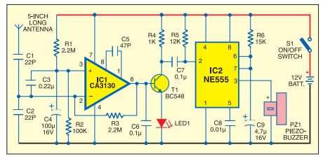
CA 3130 Op Amp
It is excellent Op Amp that requires very low input current requirements. Its output will be in the zero state in the off mode. CA3130 is the 15MHz BiMOS IC with MOSFET inputs and a bipolar output. MOSFET transistors are present in the inputs that provide very high input impedance. The input current can be as low as 10pA. The IC shows very high speed of performance and combines the advantage of both CMOS and bipolar transistors. The presence of PMOS transistors at the inputs results in common mode input voltage capacity down to 0.5 volts below the negative rail. So it is ideal in single supply applications.
The output has CMOS transistor pair that swings the output voltage within 10mV of either supply voltage terminal. IC CA3130 works off 5 to 16 volts and can be phase compensated with a single external capacitor. It also has terminals to adjust the offset voltage and strobing.
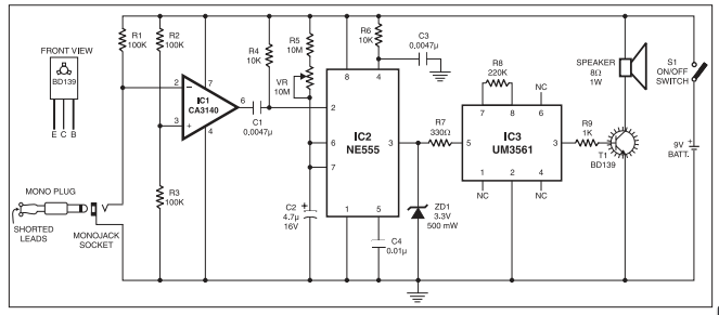
CA 3140 Op Amp
It is the 4.5MHz BiMOS Op Amp with MOSFET inputs and bipolar output. It has both PMOS transistors and high voltage bipolar transistors inside. Is inputs have gate protected MOSFETs (PMOS) that provides very high input impedance typically around 1.5T Ohms. The input current requirement is very low around 10pA. It exhibits very fast response and high speed of performance. The output has protection against damage from load terminal shorting. The input stage has PMOS FET which helps in common mode input voltage capability as low as 0.5 volts. The IC is internally phase compensated for stable operation. It also has terminals for additional frequency roll off and offset nulling.
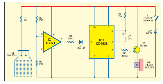
TL071 Op Amp
It is a low noise Op Amp with JFET inputs. It operates in wide common mode and consumes very little current. It requires very low input bias and offset currents. It’s output is short circuit protected and has very high slew rate of 13 V/us and exhibits latch free working.TL0 71 is ideal for high fidelity and audio preamplifier circuits. TL071 and TL0 72 contain only one Op Amp inside while TL074 is a Quad OpAmp with 4 operational amplifiers inside.
TL082 Op Amp
It is a dual OpAmp with separate inputs and outputs. It has JFET inputs and bipolar outputs. The IC shows very high slew rate, low input bias. It also has low offset current and low offset voltage. Its inputs can be biased with very low input currents. Output of the IC is short circuit protected. TL082 exhibits latch free operation and it has the internal frequency compensation.
LM 311 Op Amp
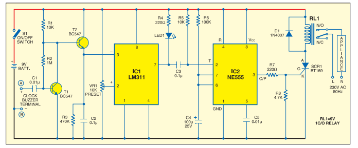
It is a single OPAMP capable of driving DTL, RTL, TTL or MOS circuits. Its output can switch up to 50 volts and 50mA current. It works on wide range of supply voltages from 5 to 30 volts and requires only single supply. It can directly drive relays, solenoids etc if the current requirement is less than 50mA.The pin connection of LM311 is different from other OpAmps. Here the pin3 is inverting input and pin2 Non inverting input. Output also is different. It has two outputs. Pin7 is the Positive output that sinks current while Pin 1 is the negative output.
Pin 7 is connected to the collector of the NPN output transistor. Pin1 forms the emitter of output transistor. Normally the output transistor is in the off state and its collector will be pulled to Vcc. If its base gets more than 0.7 volts, it saturates and turns on. This sinks current and the load turns on. So unlike other OpAmps, LM311 sinks current and output turns low when triggered.
IC 747
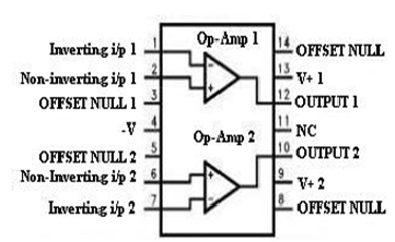
The 747 is a general purpose dual operational amplifier containing two 741 op-amps. The two operational amplifiers have a common bias network and power supply leads. Otherwise, their operation is completely independent. The characteristics of the op-amp are no latch-up when input common mode range is exceeded, freedom from oscillations. It is a 14-pin dual in line package (DIP), shown in figure below:
Pin Description of 747 Op-amp:
Pin1 - Inverting input terminal of op-amp1
Pin2 - Non-inverting input terminal of op-amp1
Pin3 - Offset null terminal op-amp1
Pin4 - Negative supply voltage (-V)
Pin5 – Offset null terminal of op-amp2
Pin6 – Non-inverting input terminal of op-amp2
Pin7 – Inverting input terminal of op-amp2
Pin8 - Offset null terminal of op-amp2
Pin9 – Positive supply voltage (+V) of op-amp2
Pin10 – Output of op-amp2
Pin11 – No connection (NC)
Pin13 – Positive supply voltage of op-amp1
Pin14 – Offset null terminal of op-amp1
Features of 747 op-amp:
- Dual supply voltage ±1.5V to ±15V
- No frequency compensation required
- Short-circuit protection
- Wide common-mode and differential voltage ranges
- Low power consumption
- Unity gain stable
- No latch-up
- Balanced offset null
- Supply current is less than 300 μA per amplifier at 5 V
How to test an Op Amp IC?
Operational Amplifiers are widely used in electronic circuits as amplifiers, comparators, voltage follower, summing amplifier etc. Most of the commonly used Op Amps like 741, TL071, CA3130, CA3140 etc have same pin configurations. Hence this tester is useful to check the working of the Op Amp during trouble shooting or servicing. It is an easy to make tool which is essential in the work bench of a hobbyist or technician.
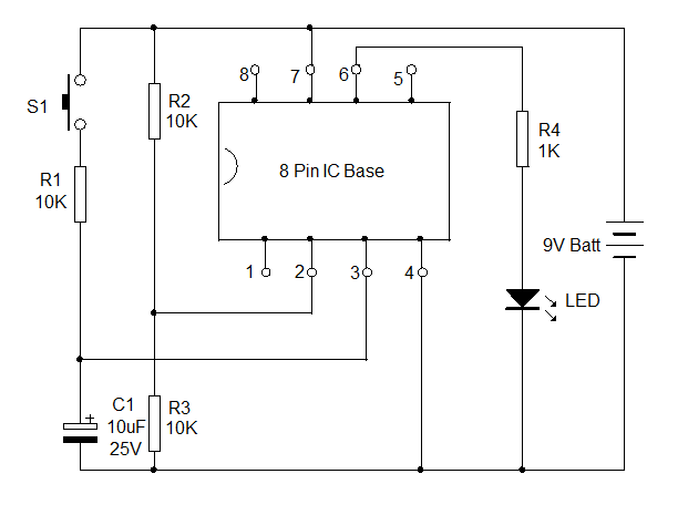
The tester is wired around an 8 pin IC base into which the IC to be tested can be inserted. Pin 2 (inverting input of IC) is connected to a potential divider R2, R3 that gives half supply voltage to pin 2. Pin 3 (None inverting input) of IC base is connected to the VCC through R1 and a Push to on switch. Output pin 6 is used to connect the visual indicator LED via the current limiting resistor R4.
The design is a voltage comparator. Insert the IC in to the socket with correct orientation. The notch at the left side of the IC should match with the notch in the IC base. In this comparator mode, the output of IC1 goes high when its pin 3 gets a higher voltage than pin 2. Here pin 2 gets 4.5 volts (if battery is 9V) and pin 3, 0 volts.
So the output remains low and LED will be dark. When S1 is pressed, pin 3 gets higher voltage than pin 2 and the output of IC turns high to light the LED. This indicates that the circuitry inside the IC is working.


No comments:
Post a Comment